Just got the board few days back, been busy to try out the board but the performance doesn’t seem any surprise or out of expectation, or may be worst than p35 chipset, I hope it can be solve via bios, lets have a look at real “item”
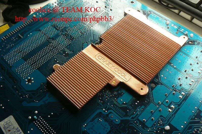
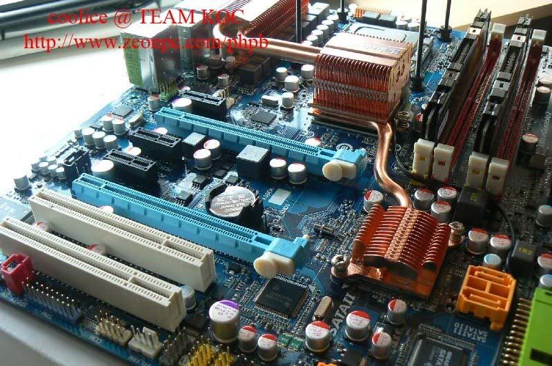
the “Crazy Cool” backplate
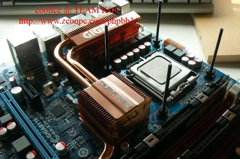
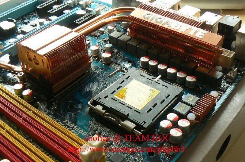
CPU area
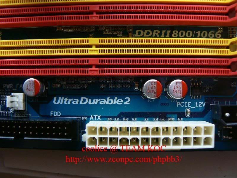
Dual x16 PCI-E
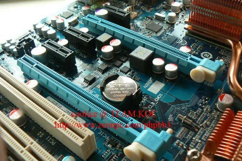
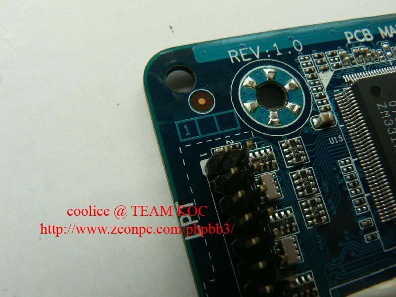
PCB Made in Taiwan
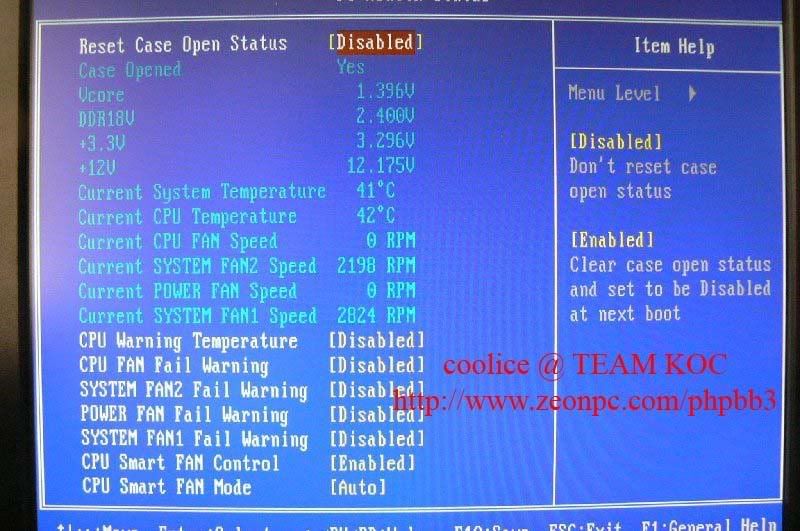
p/s: note tat ITE chipset, our software temperature sensor get reading from here
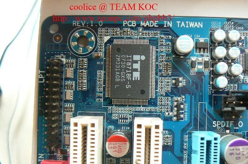
6 Layers PCB which help in dissipating heat
Ultra Durable2..does it work?lol
I stick a thermal probe at the base of heatpipe cooler
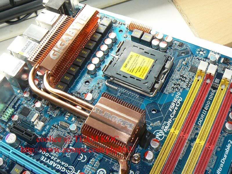
the heatpipe cooler really improve a lot from previous one, much better I would say,but still..x38 very hot
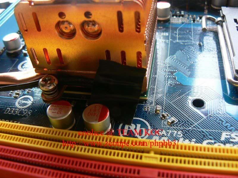
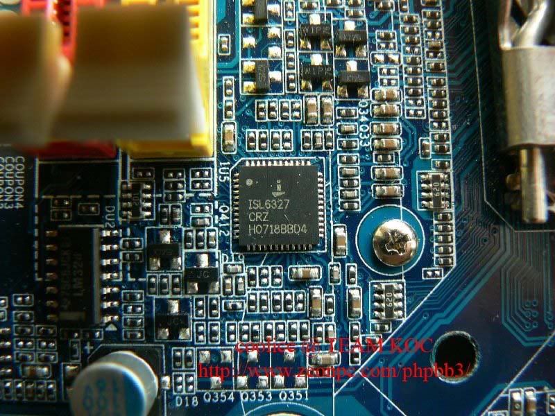
Voltage regulator
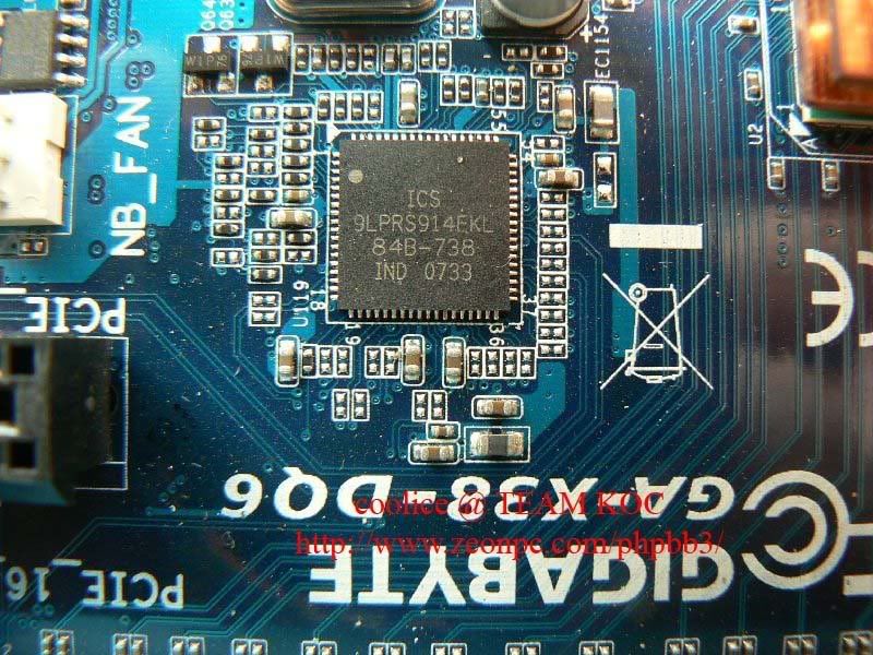
Clockgen
Fixed up with watercooling mounting and ready to test
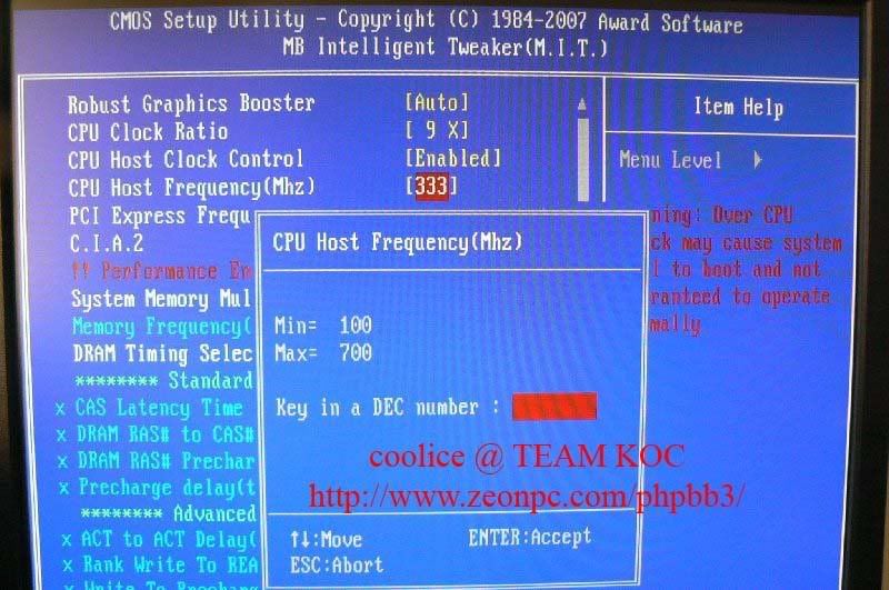
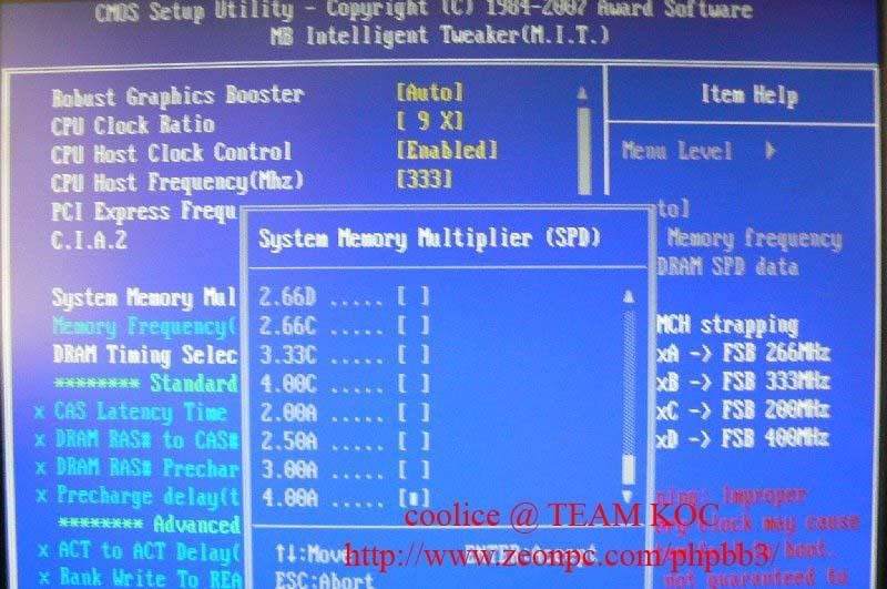
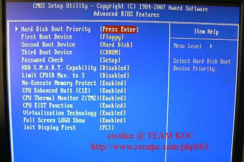
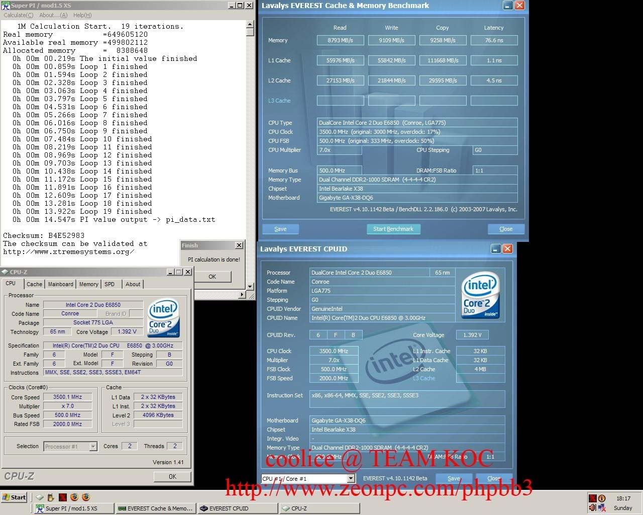
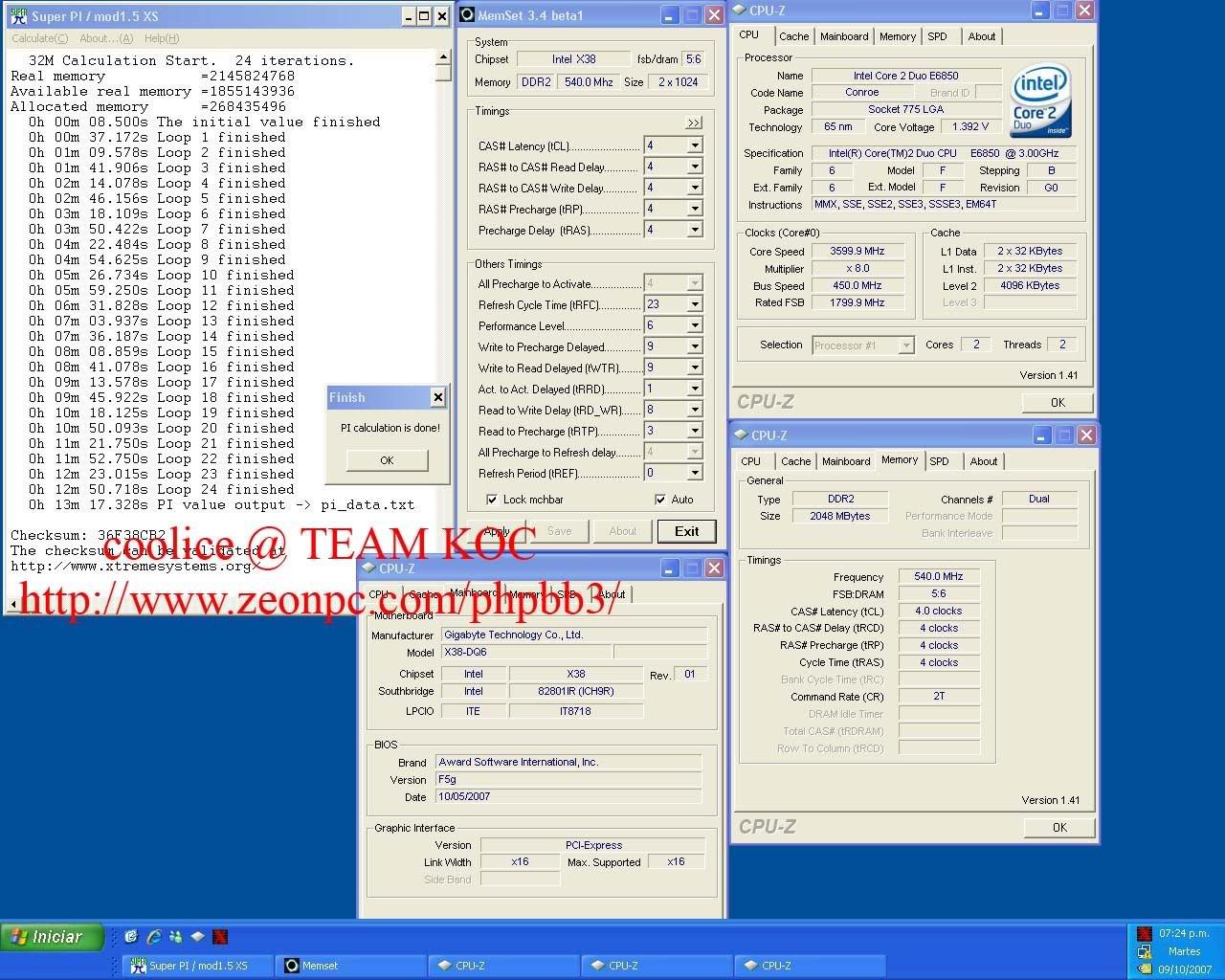
First of all, look at the bios first
M.I.T
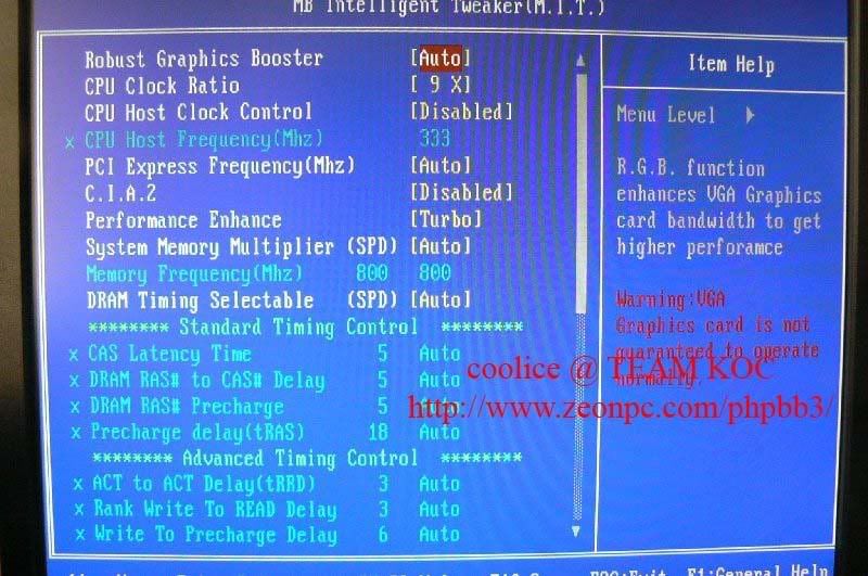
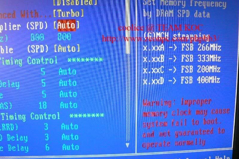
FSB(100~700)
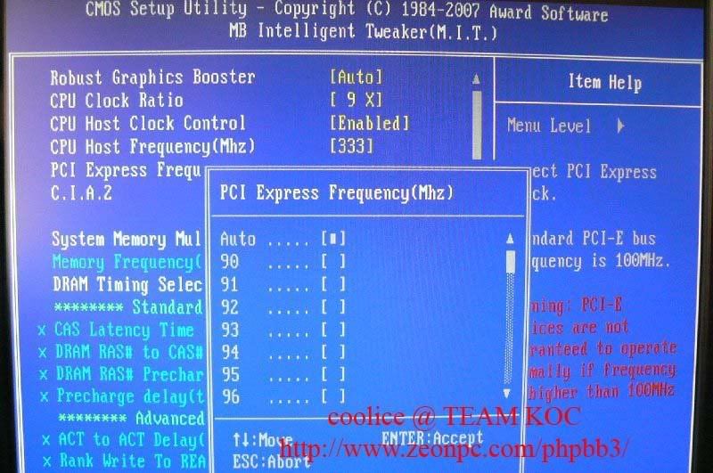
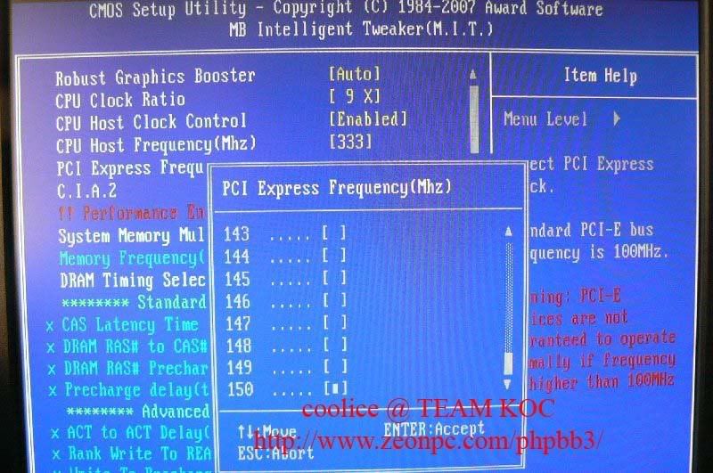
PCIE Frequency
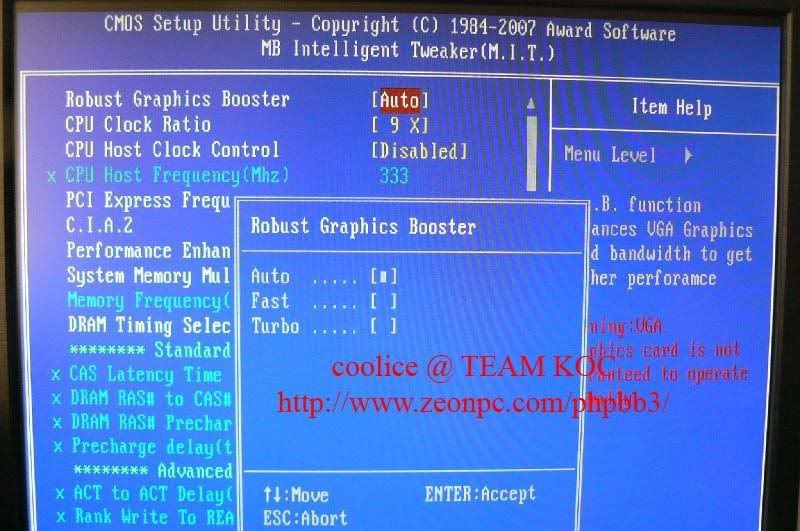
Robust Graphics Booster
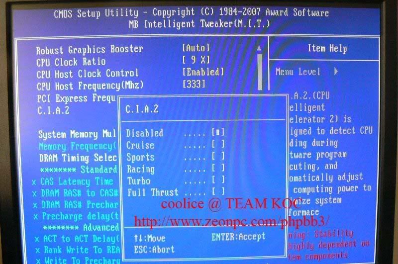
C.I.A.2
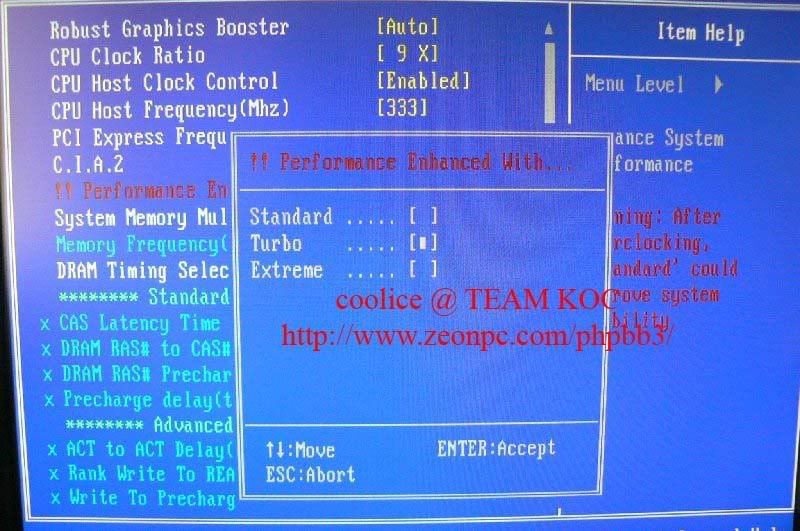
Performance Enhance
set to extreme can gain some little bandwidth
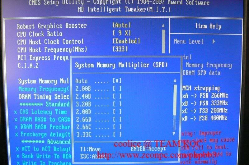
Strap tied with ram divider
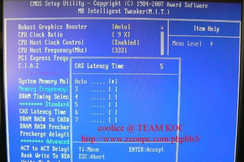
CAS Latency Time(3~7)
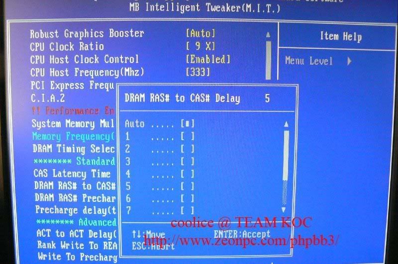
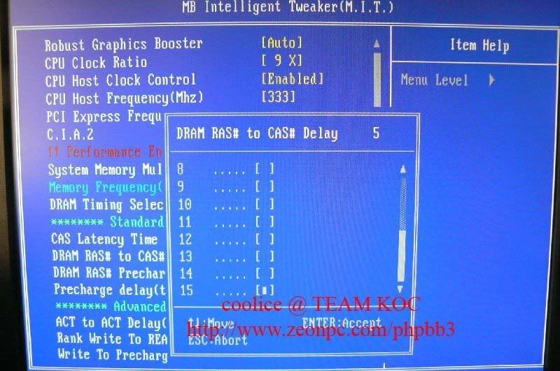
RAS# to CAS# Delay(1~15)
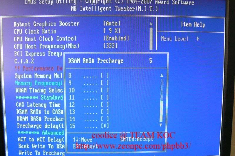
RAS# Precharge(1~15)

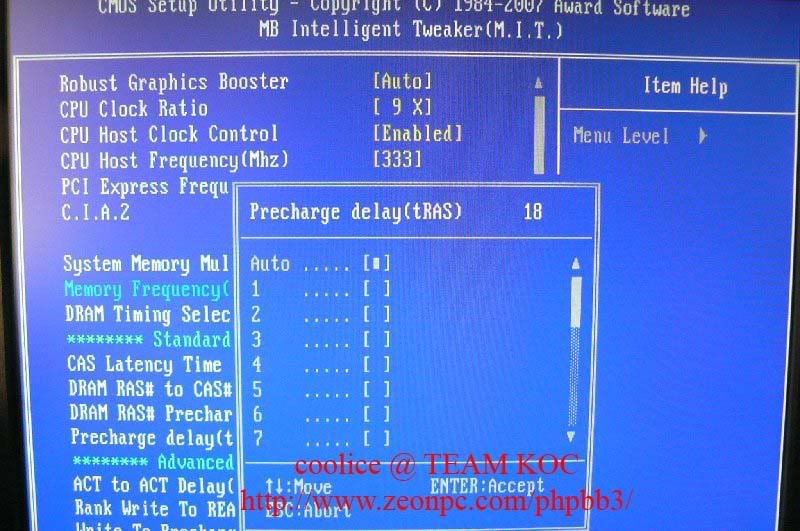
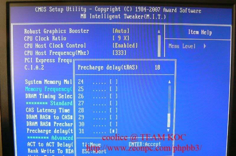
tRAS(1~31)
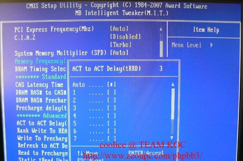
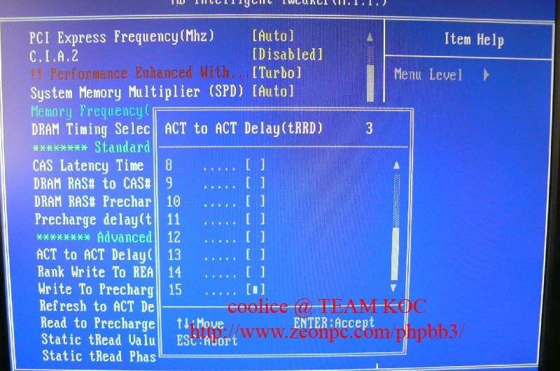
tRRD(1~15)
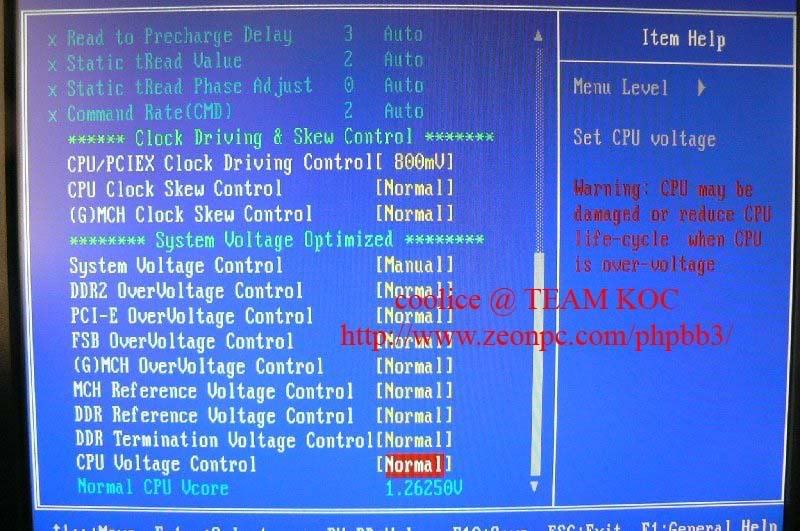
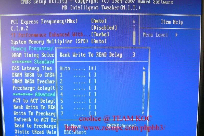
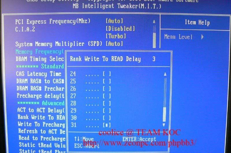
Write to READ Delay(1~31)
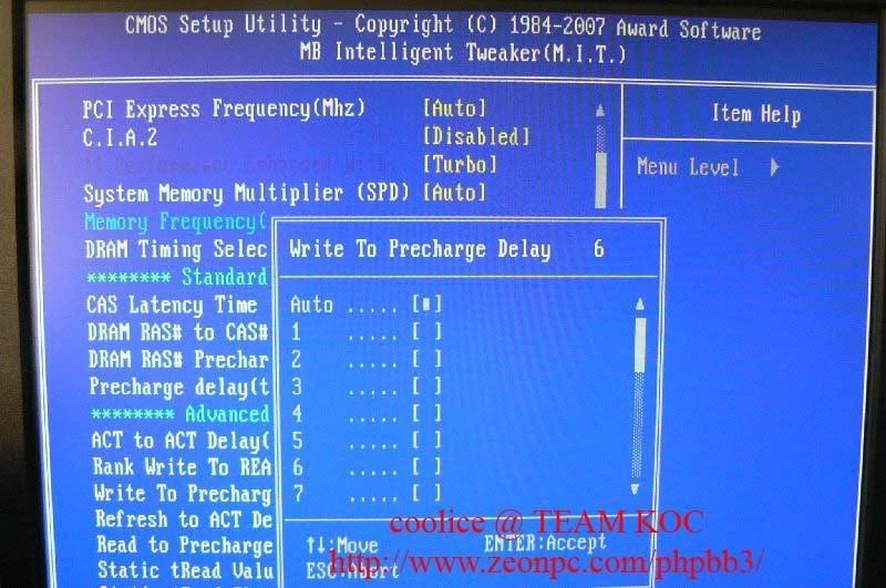
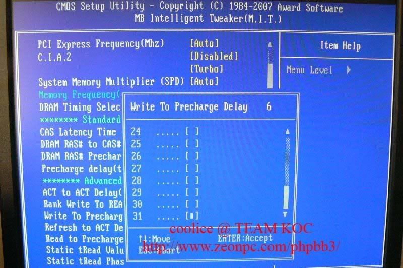
Write to Precahrge Delay(1~31)
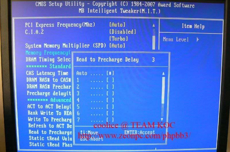
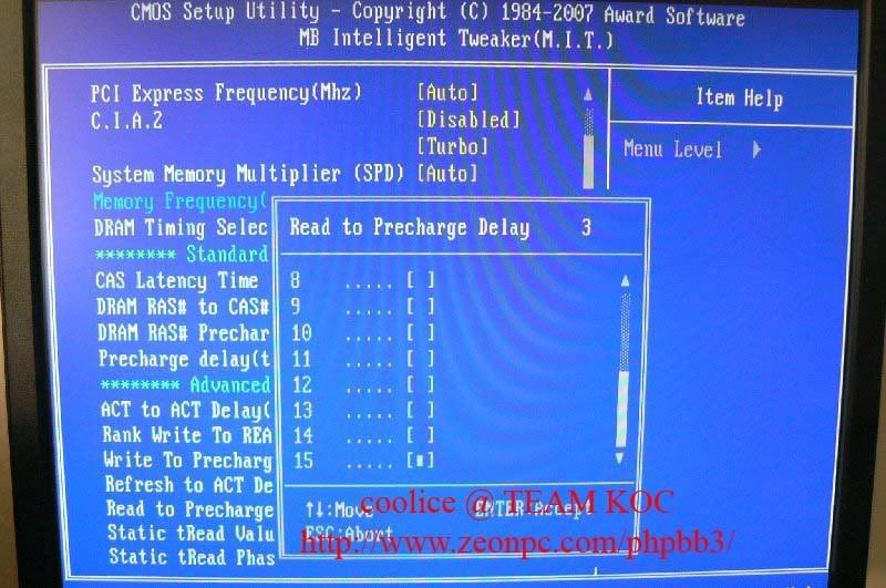
Read to Precharge Delay(1~15)
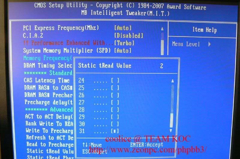
tRD(1~31)
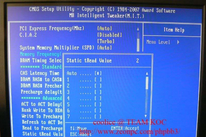
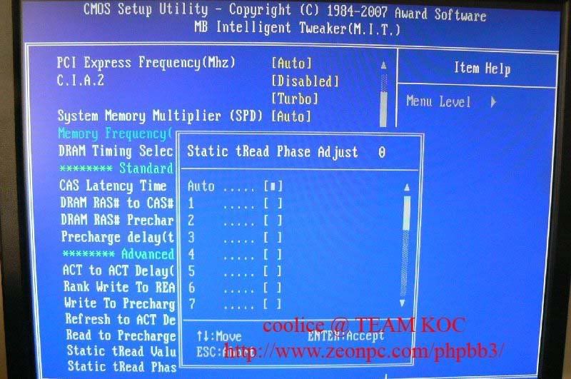
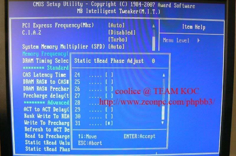
Static tRead Phase Adjust(1~31)
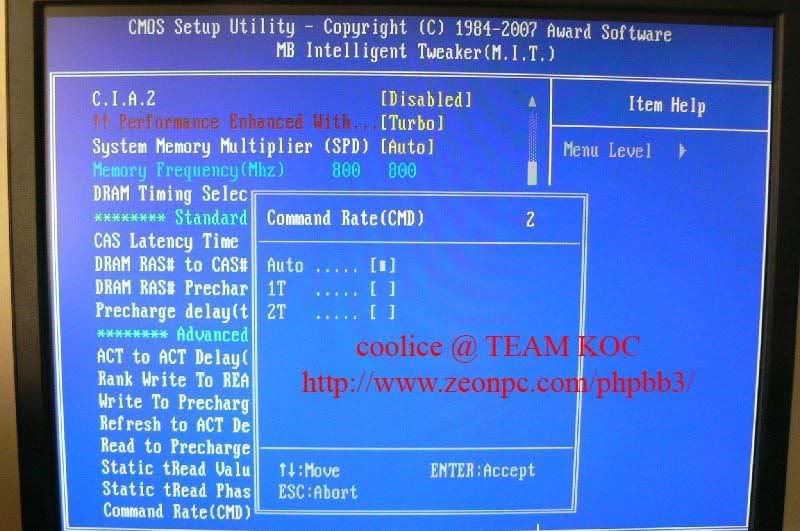
CMD Rate
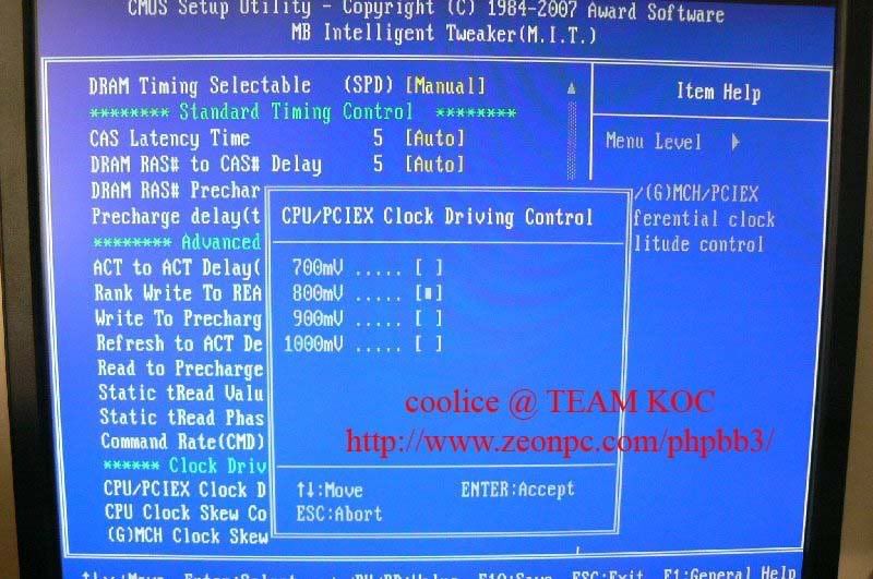
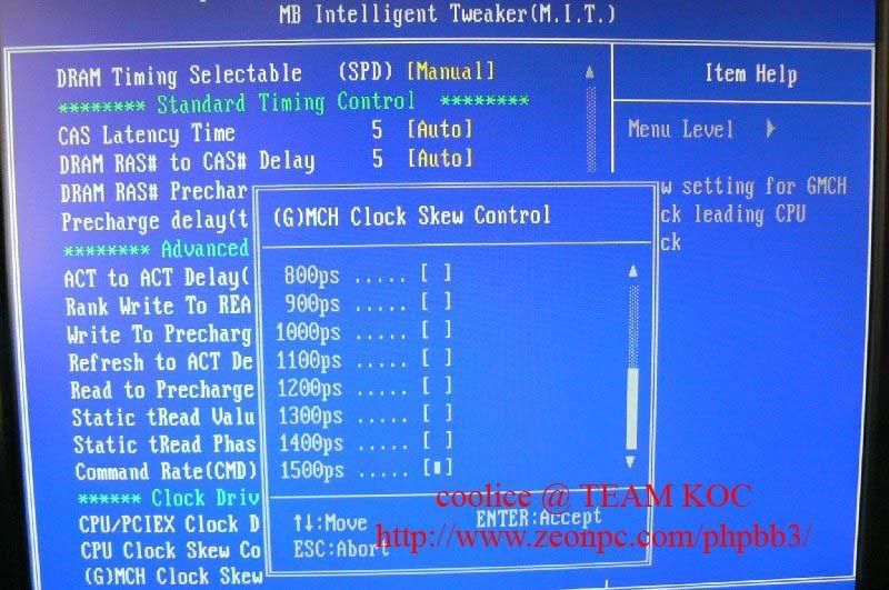
it doesn’t work in F3 bios
CPU/PCIEX Clock Driving Control
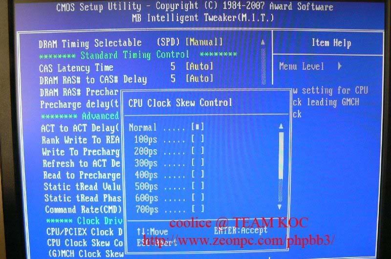
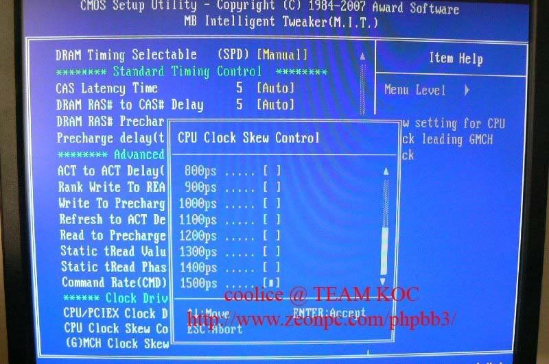
CPU Clock Skew Control
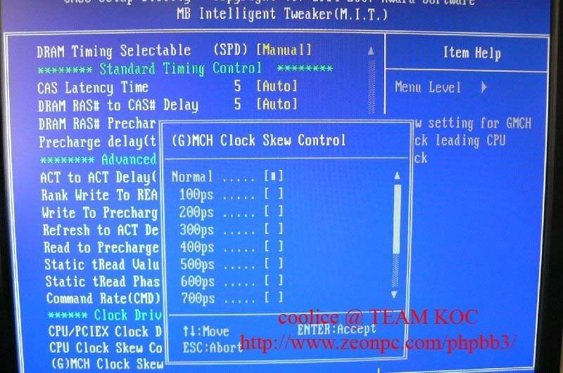
MCH Clock Skew Control
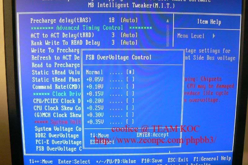
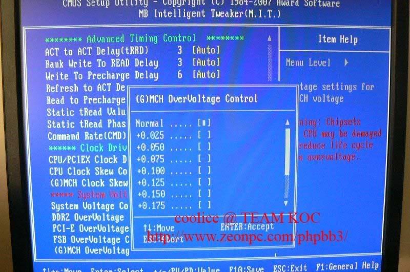
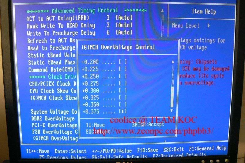
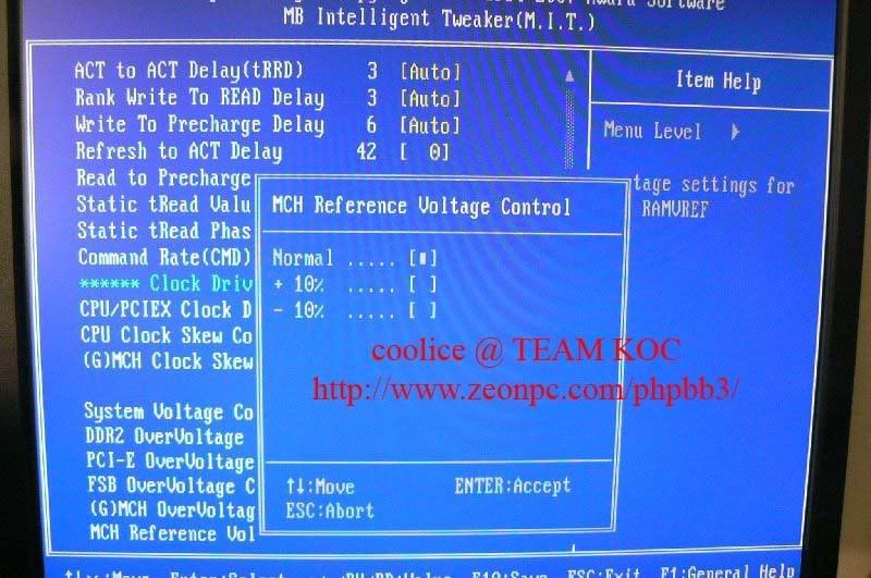
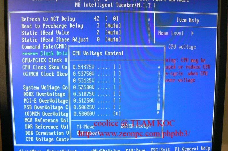
Voltage Freak?
VDimm
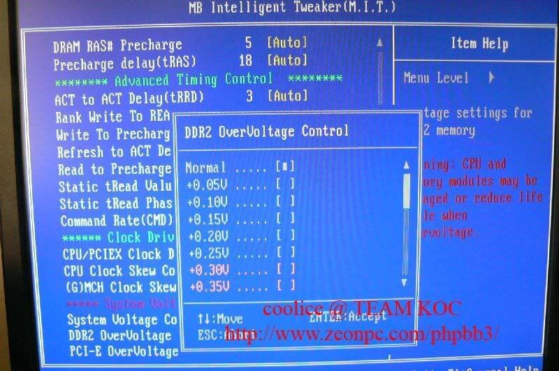
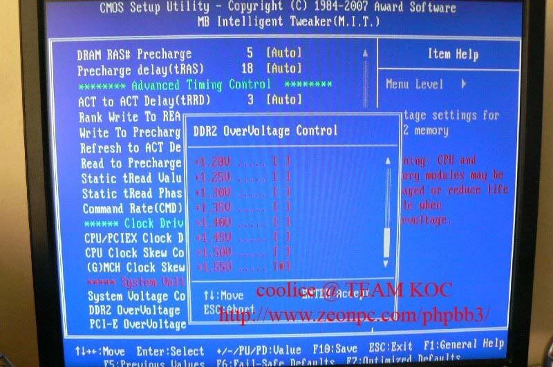
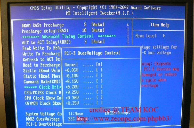
PCI-E Voltage tied together with vPLL
vFSB
vMCH
MCH Ref Volt Control
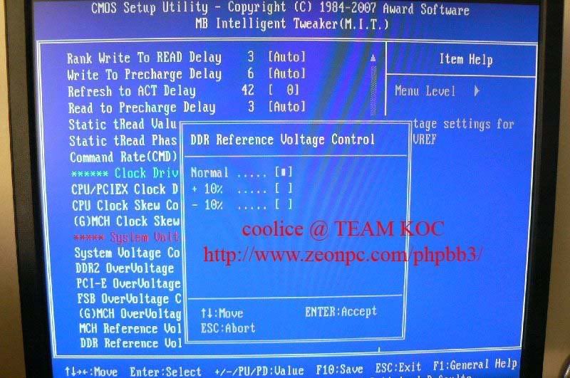
DDR Ref Volt Control
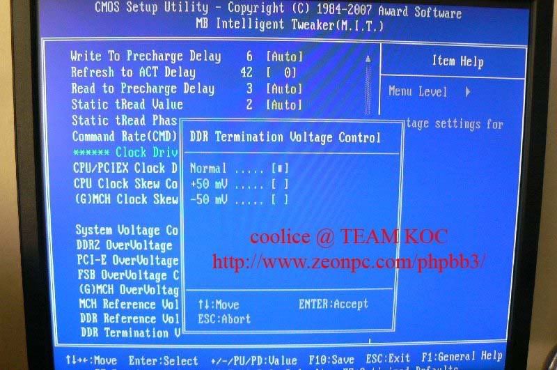
MCH Termination Volt Control
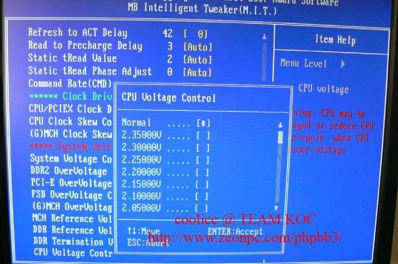
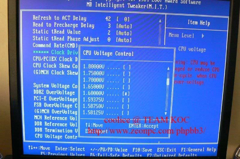
VCore
CPU Feature
switch them off if u r overclock
thanks for viewing and sorry abt my english and the pic abit cacat after compressed by imageshack
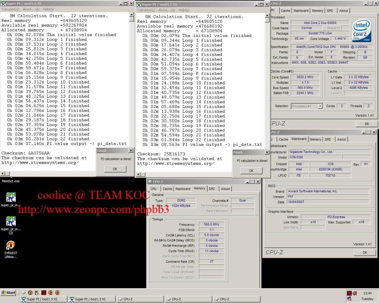
system spec
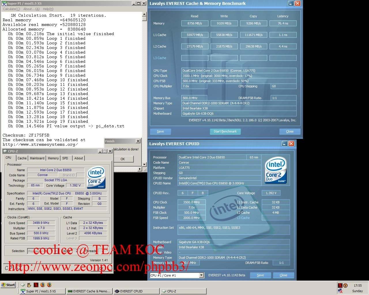
C2D E6850 watercooled
Team Xtreem / Crucial 10th anny 1GB x2
nVidia 7300gt
silverstone op650 / op1000
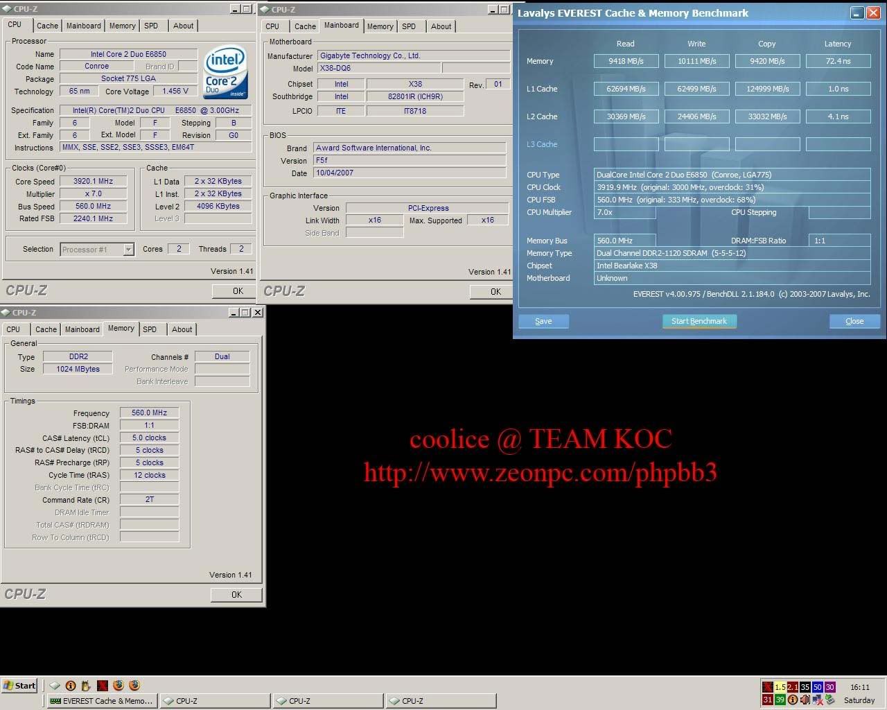
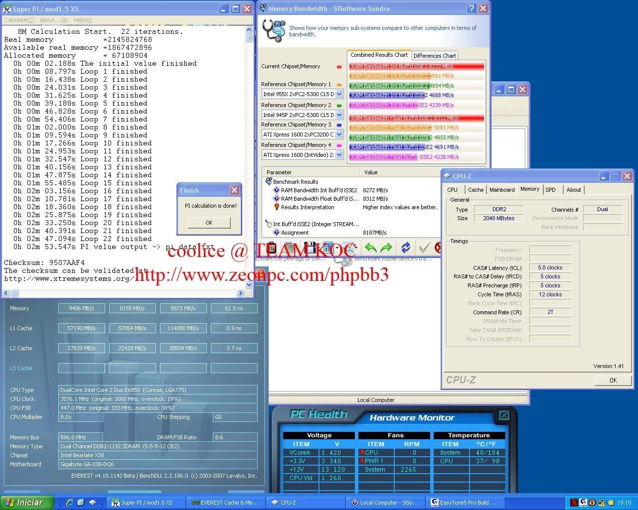
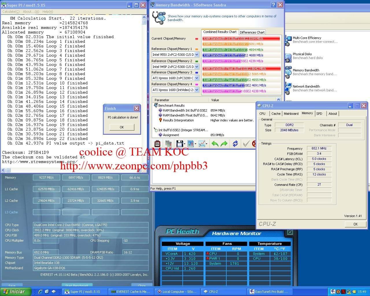
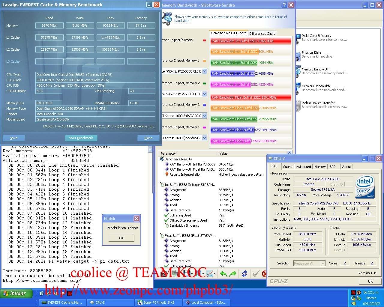
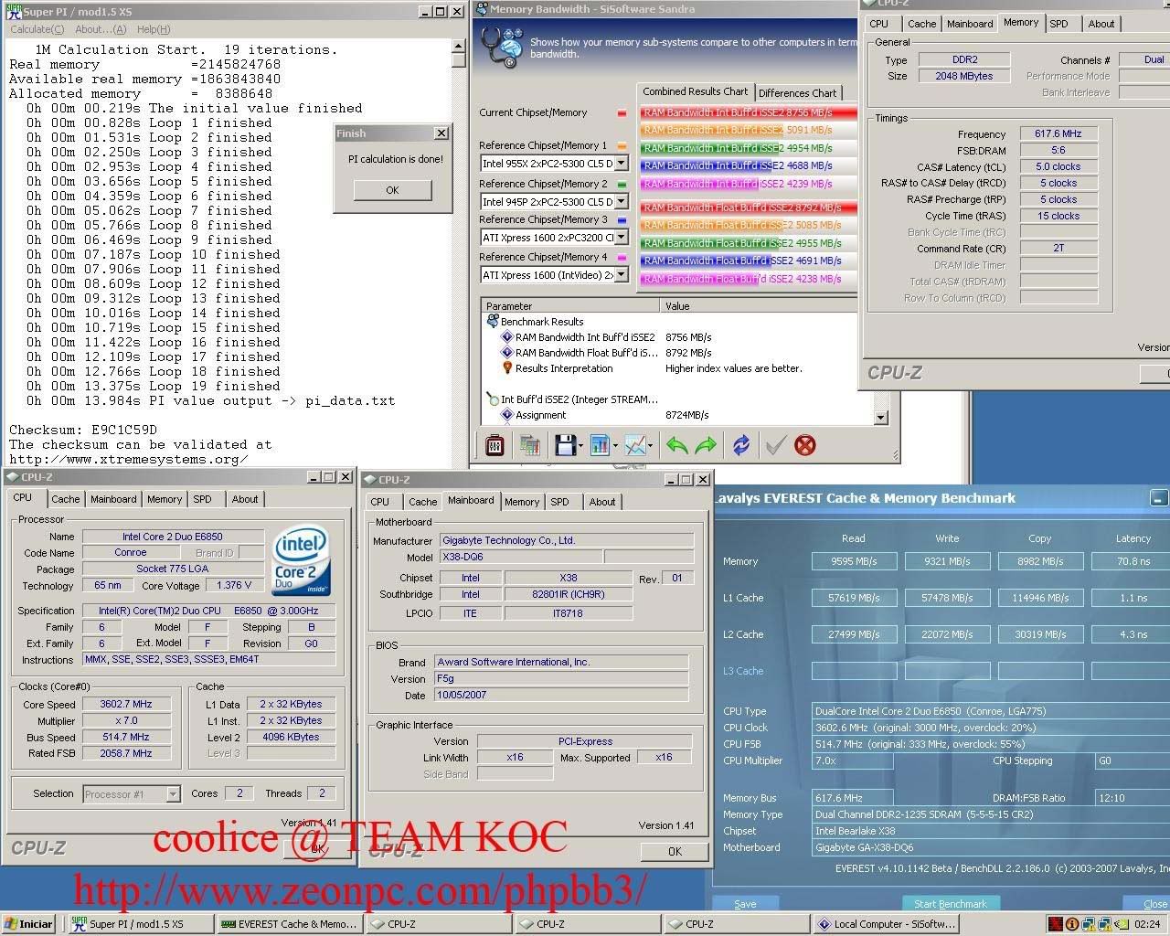
P/S: this is F5f bios
Performance Enhance
Standard
Turbo
Xtreme
Turbo and Xtreme mode give a some performance boost but I unable to get it stable with Xtreme when running ddr1300 5-5-5-12
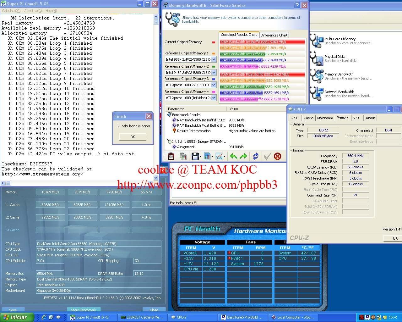
485x7
1:1 266 strap
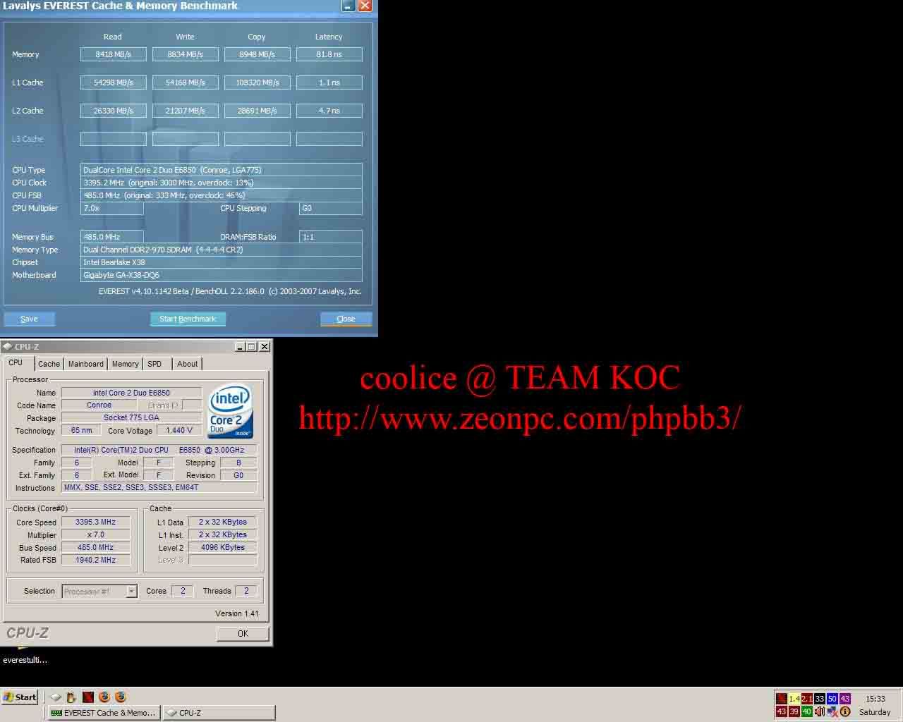
1:1 333 strap

1:1 400 strap

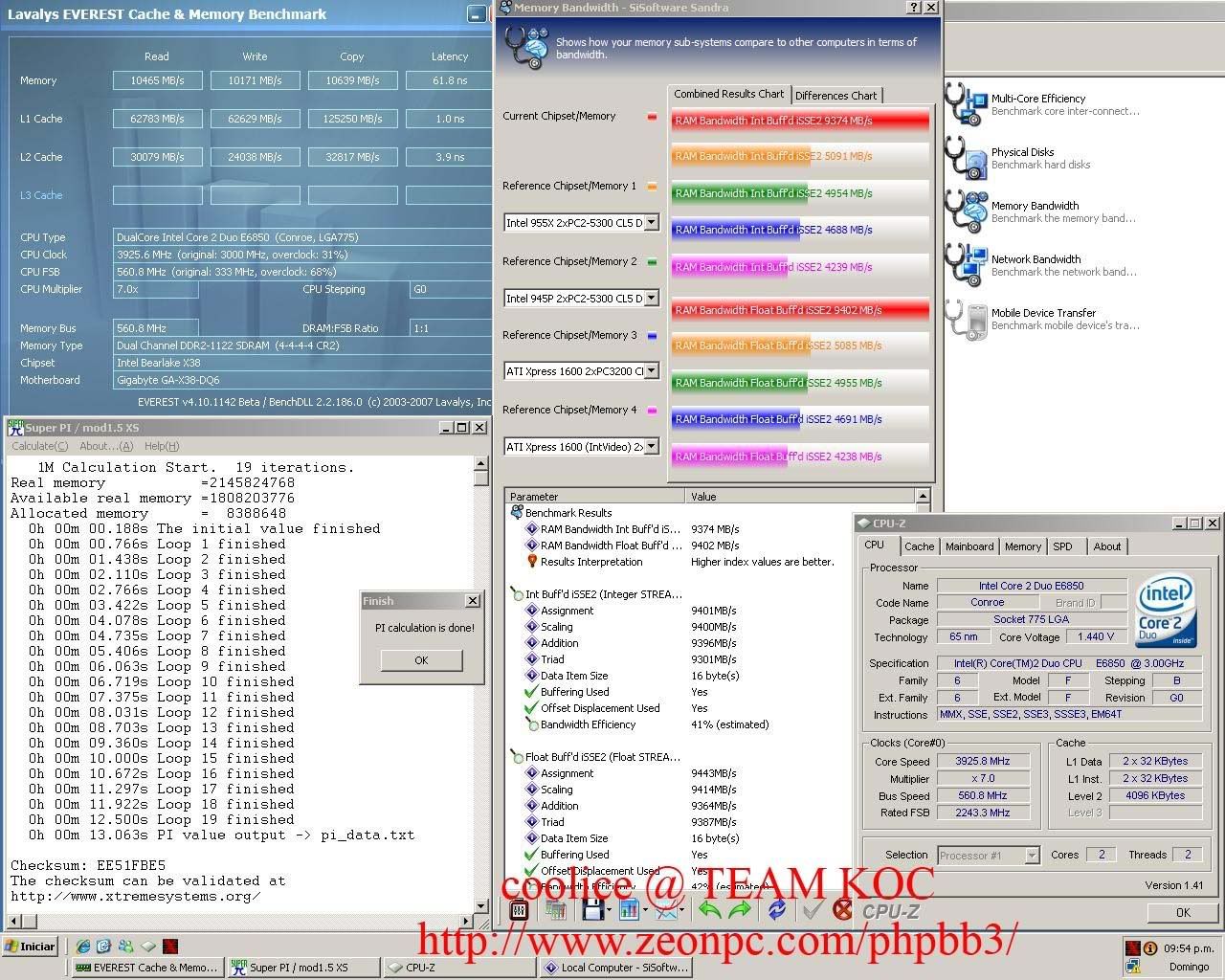
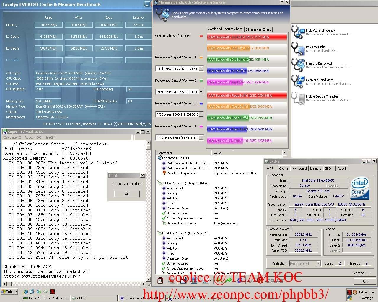
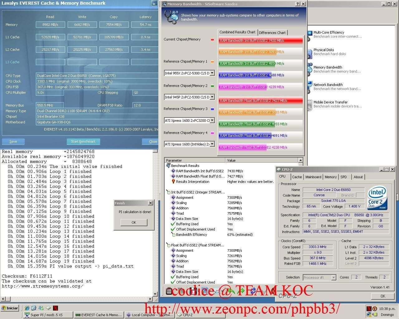
Comparing between straps, I cant do high fsb if 266 strap was selected but with 333 and 400 strap, I can do up to 560fsb and tat is also my proc highest fsb
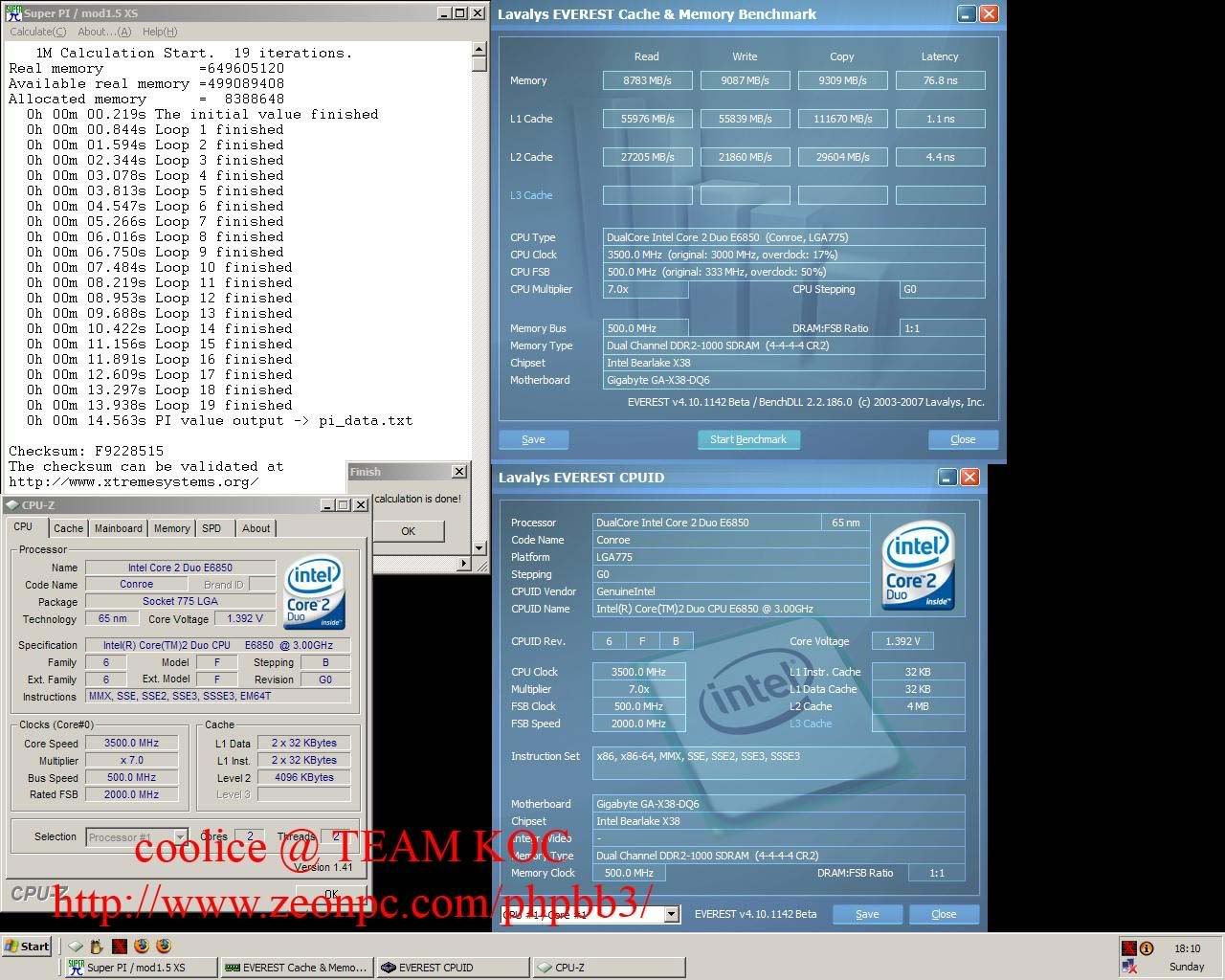
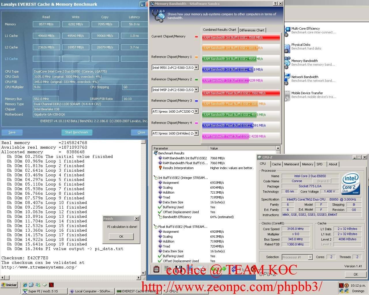
This is running at 550x7 with 400 strap and latter with 333 strap


5:6 divider 333strap

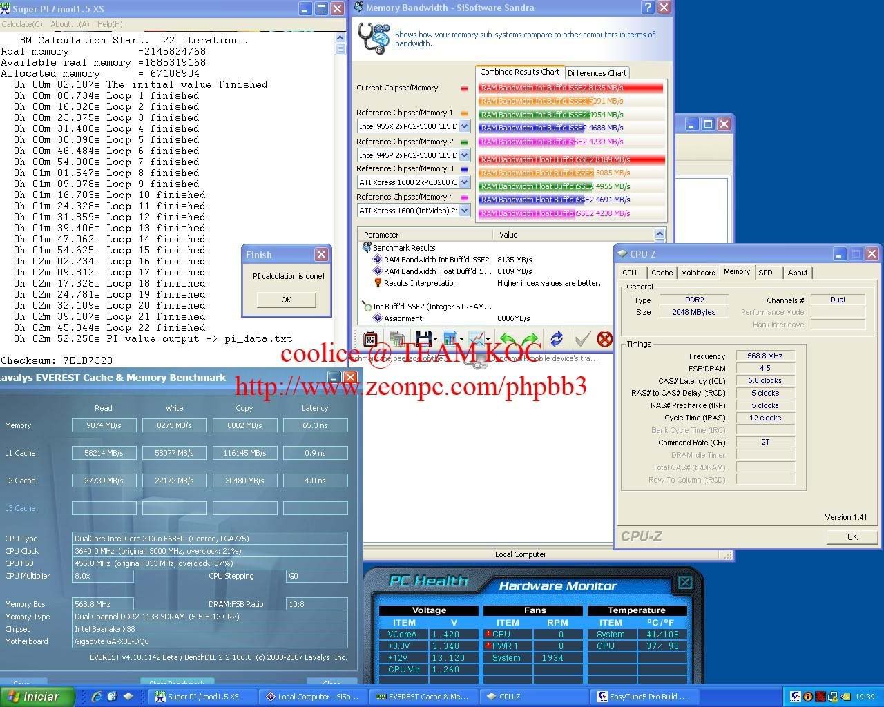
4:5 divider 266strap

New divider 3:4 400strap
3:4 200strap

200 strap give better bandwidth and latency


Clockspeed does affect bandwidth huh?
2:3 divider 266strap

5:8 divider 333 strap

Again clockspeed does affect bandwidth ?
3:5 divider 200strap

1:2 divider 266strap and 200strap


Not much different
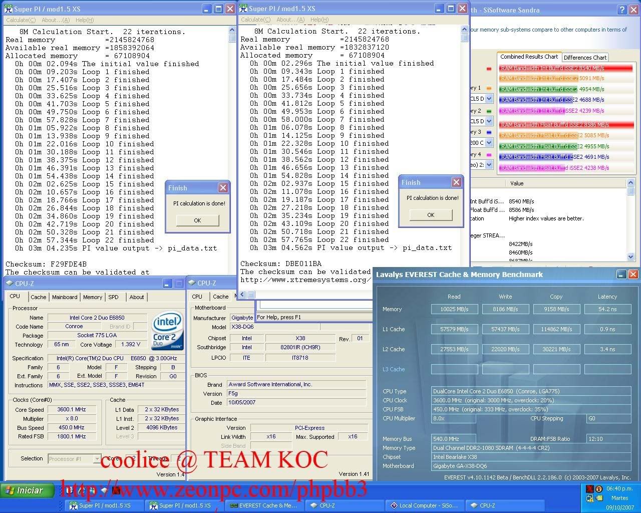
Highest fsb 560x7
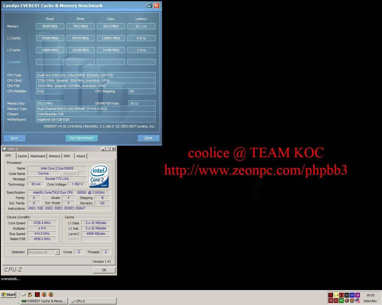
Try with 10th anny this time
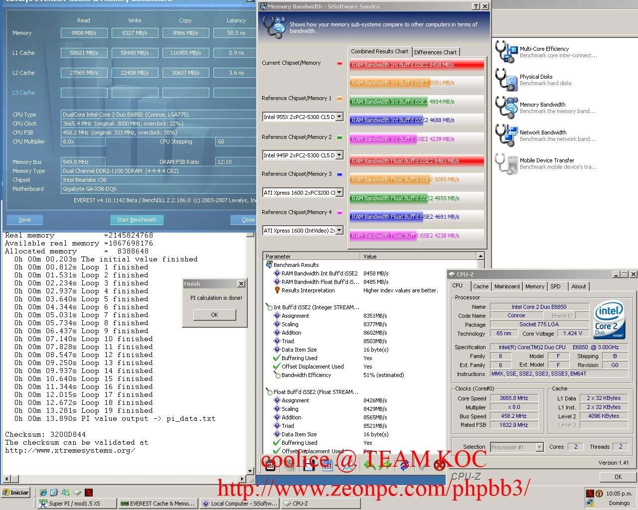
Ok..i heard tat quite a lot of them saying f3 the best bios..so I give it a try
Again my highest fsb,take it compare with F5f bios above,1k MB/s reading bandwidth and 10ns latency gain
1:1 divider
5:6 divider
4:5 divider
2:3 divider
5:8 divider
3:5 divider
1:2 divider 200 strap
1:2 divider 266strap

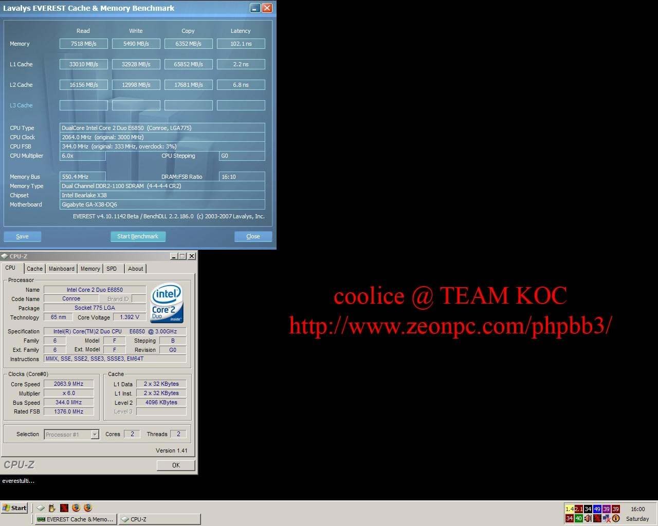
In F3 bios,the 3:4 divider is missing and also only 1:2 divider come with 2 diff strap selection
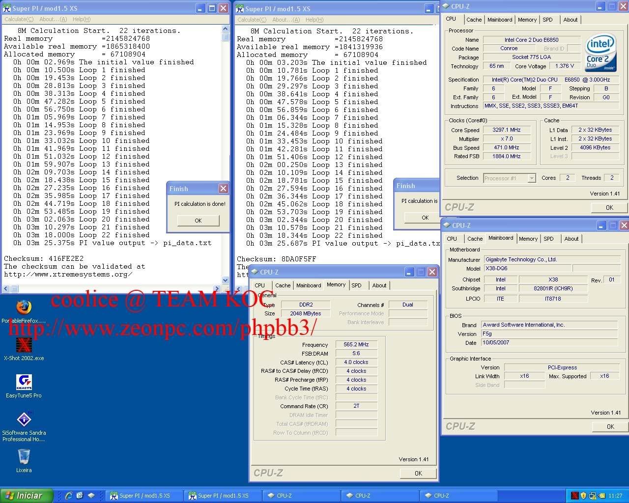
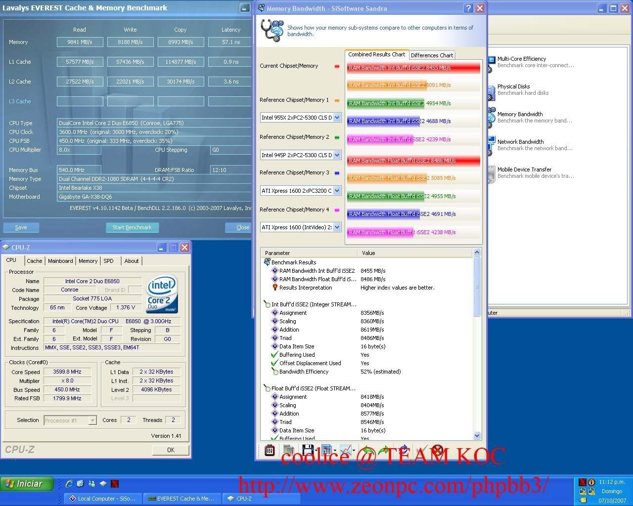
New bios out,F5g…hehe..lets see 450x8
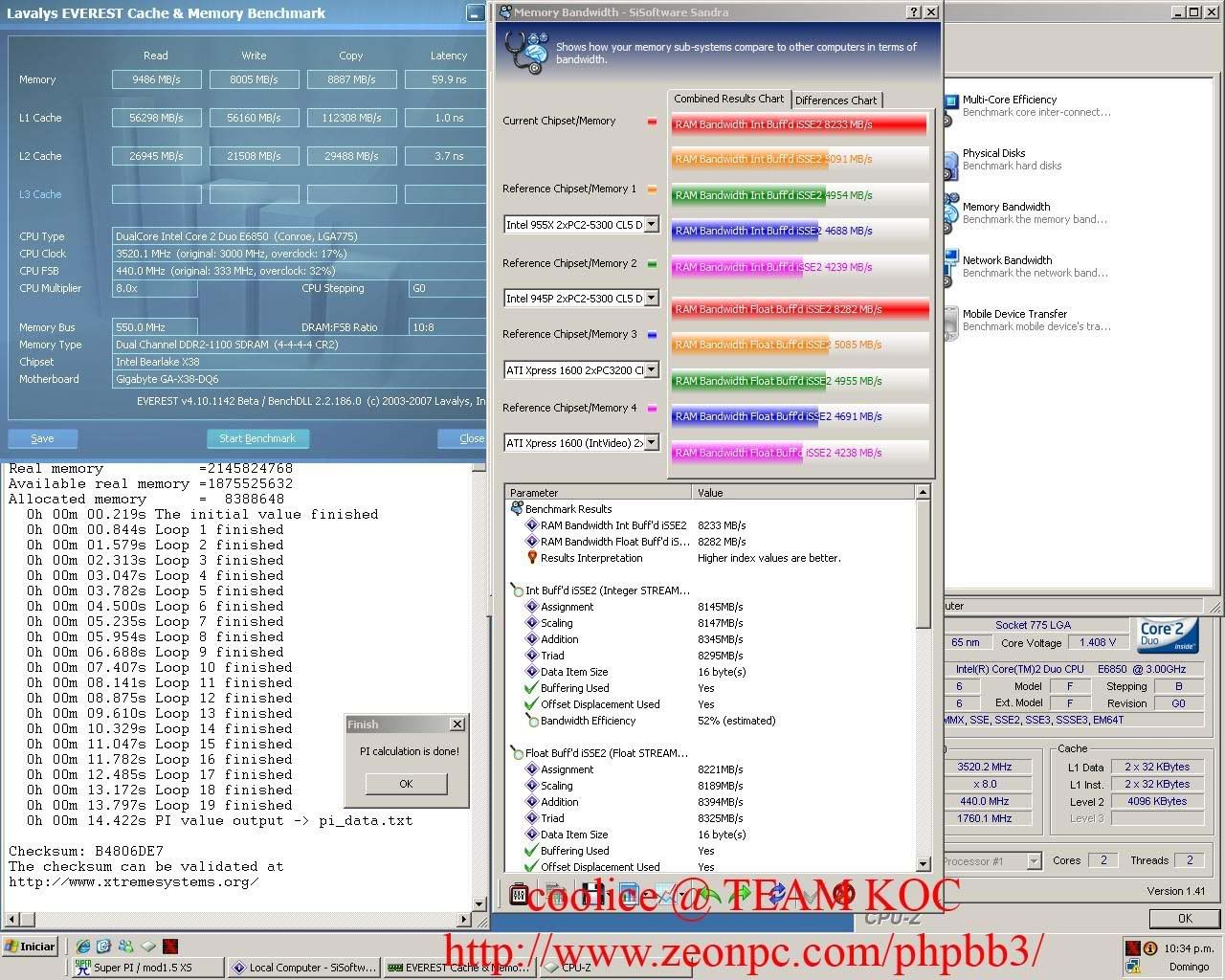
F3
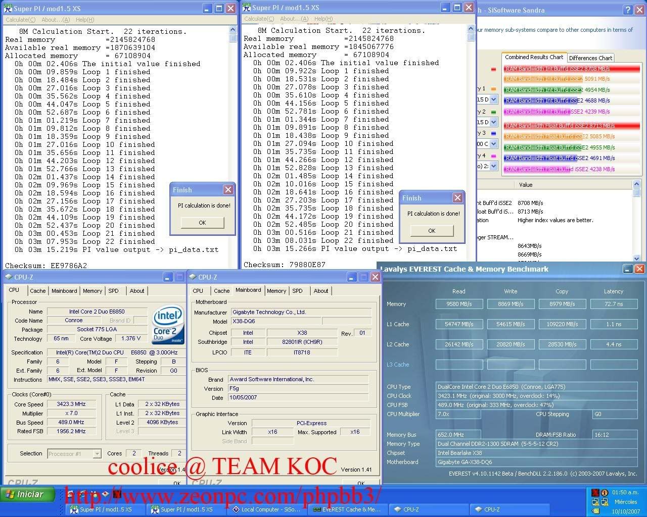
F5g
Trying highest fsb can go with diff strap
333 strap,limited by ram,but np to do 560x7 at 333strap 1:1 divider
266strap,max fsb 455
200strap max fsb 447
400strap..limited by ram again..hehe
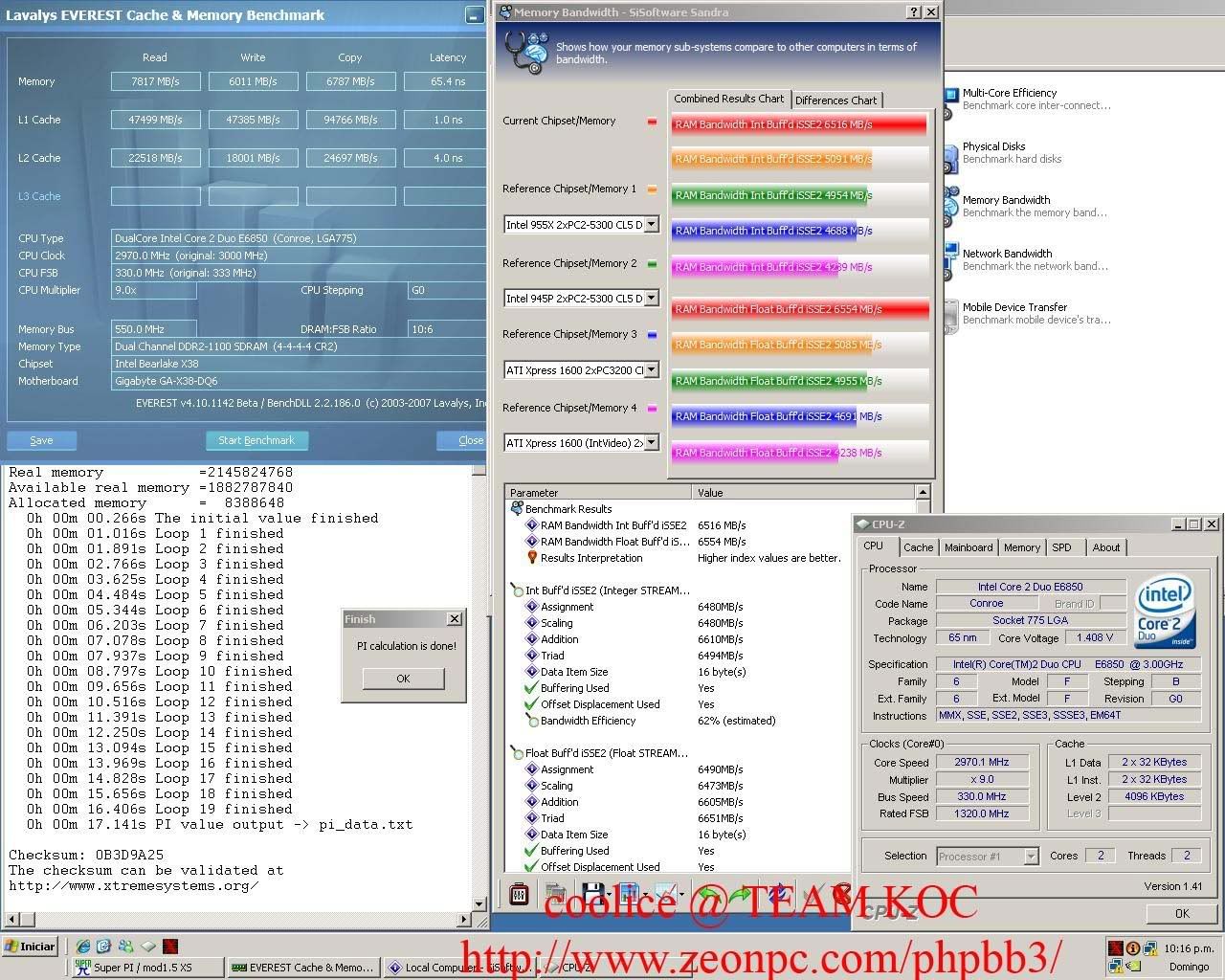
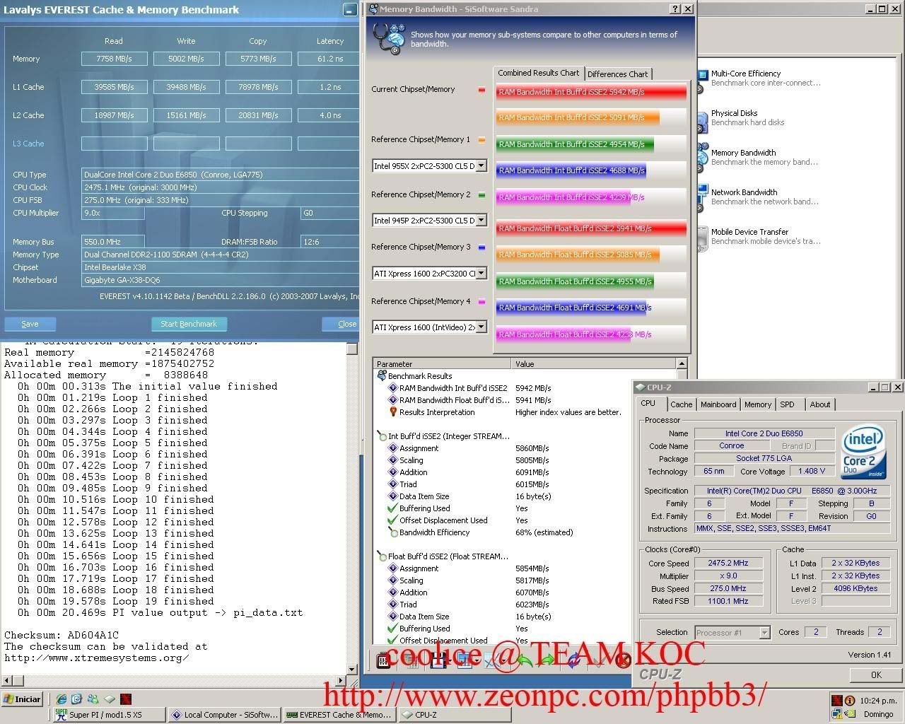
Some other result
*When I do comparing between dividers,ram speed always ddr1100 4-4-4-4


